
Payment Type:T/T
Incoterm:FOB,CIF,EXW
Min. Order:50 Piece/Pieces
Transportation:Ocean,Air,Express
Port:NINGBO,SHANGHAI
$0.2-10 /Piece/Pieces
Place Of Origin: China
Transportation: Ocean,Air,Express
Place of Origin: CHINA
Certificate: ISO9001:2015 / ISO14001:2015
Port: NINGBO,SHANGHAI
Payment Type: T/T
Incoterm: FOB,CIF,EXW
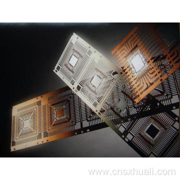
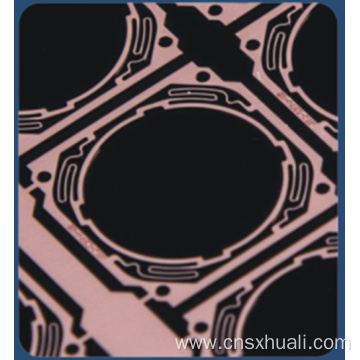
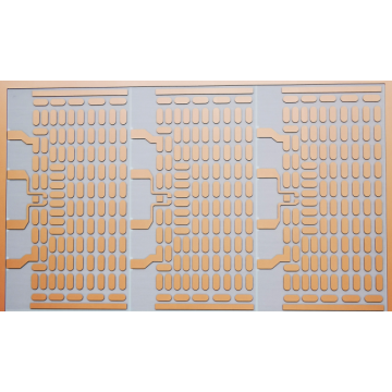
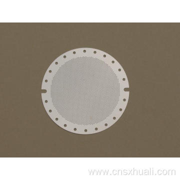
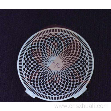
Custom Etch DBC Substrate for High-speed Rail
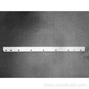
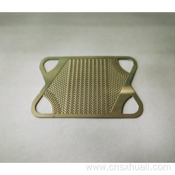
DBC Substrate mainly used in the fields of rail transit, smart grid, new energy vehicles, industrial frequency conversion, household appliances, military power electronics, wind and photovoltaic power generation. DBC (Direct Bonded Copper) Substrate is a special process board where copper foil is bonded directly to the surface (single or double sided) of and AI203 OR AIN ceramic substrate at high temperatures and can be etched with various graphics. The products have many superiorities, for example, it is highly resistant to vibration and wear, ensuring its long service life. Also, A large number of high-voltage, high-power devices have high requirements for heat dissipation, and ceramic substrates have a better heat dissipation effect. Moreover, it has excellent electrical insulation performance, excellent soft brazability, high adhesion strength and a large current-carrying capacity.
We custom High Precision DBC Substrate with drawings provided by customers. The raw material we use for Etched DBC Substrate is Ceramic-based double-sided copper clad laminate. We are equipped with professional metal etching equipment and exposure development equipment. Our etching process can achieve Double-Sided Etching of different graphics with 0.3 mm - 0.8mm thickness of copper clad laminate. Also, we can guarantee that our Double-Sided Copper Clad Laminate Substrate is neatly arranged, straight surface line, and have no burr, high product accuracy.
Below are the specific parameters of this product, please check more Semiconductor Chip Carrier in our website for more ideas.
| Material | Thickness of Copper Clad Laminate | Manufacturing Capacity Minimum Spacing | Manufacturing Capacity Side Corrosion |
| Ceramic-based Double-sided Copper Clad Laminate | 0.3 mm - 0.8mm | 0.5 mm - 1.2mm | 0 mm - 0.3mm |
Etch DBC Substrate