
Payment Type:L/C,T/T
Incoterm:FOB,CIF,EXW
Min. Order:50 Piece/Pieces
Transportation:Ocean,Air,Express
Port:NINGBO,SHANGHAI
$0.2-10 /Piece/Pieces
Place Of Origin: China
Transportation: Ocean,Air,Express
Place of Origin: China
Certificate: ISO9001:2015 / ISO14001:2015
Port: NINGBO,SHANGHAI
Payment Type: L/C,T/T
Incoterm: FOB,CIF,EXW
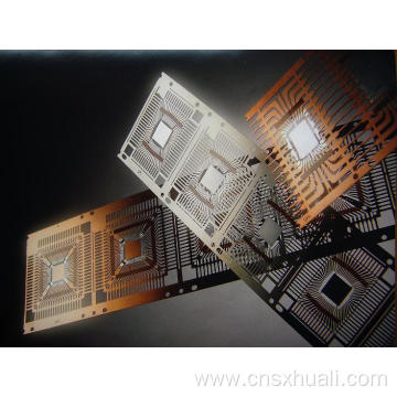
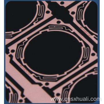
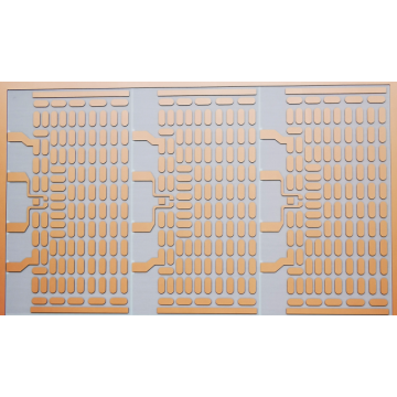
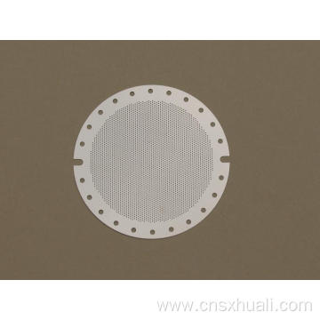
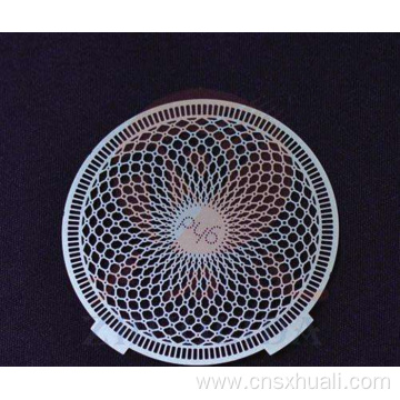
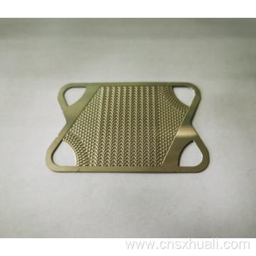
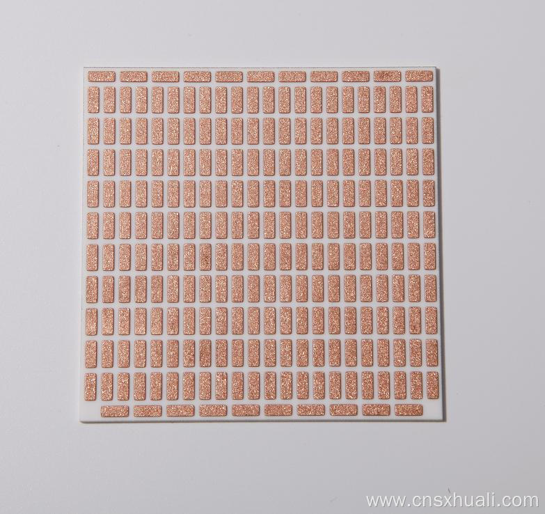
DBC (Direct Bonded Copper) Substrate is a special process board where copper foil is bonded directly to the surface (single or double sided) of and AI203 OR AIN ceramic substrate at high temperatures and can be etched with various graphics. It has excellent electrical insulation performance, high thermal conductivity, excellent soft brazability, high adhesion strength and a large current-carrying capacity. DBC Substrate mainly used in the fields of rail transit, smart grid, new energy vehicles, industrial frequency conversion, household appliances, military power electronics, wind and photovoltaic power generation.
We custom High Precision DBC Substrate with drawings provided by customers. The raw material we use for Etched DBC Substrate is Ceramic-based double-sided copper clad laminate. We are equipped with professional metal etching equipment and exposure development equipment. Our etching process can achieve Double-Sided Etching of different graphics with 0.3 mm - 0.8mm thickness of copper clad laminate. Also, we can guarantee that our Double-Sided Copper Clad Laminate Substrate is neatly arranged, straight surface line, and have no burr, high product accuracy.
Its superiorities of DBC Substrate are as follow:
1. A ceramic substrate with a coefficient of thermal expansion close to that of a silicon chip, which saves the transition layer of Mo chips, saving labour, material and cost.
2. Excellent thermal conductivity, making the chip package very compact, thus greatly increasing the power density and improving the reliability of systems and devices.
3. A large number of high-voltage, high-power devices have high requirements for heat dissipation, and ceramic substrates have a better heat dissipation effect.
4. Ultra-thin (0.25mm) ceramic substrates can replace beo, without environmental toxicity problems.
5. Large current carrying capacity, 100A continuous current through 1mm wide 0.3mm thick copper body, temperature rise of about 17 ℃; 100A continuous current through 2mm wide 0.3mm thick copper body, temperature rise of only about 5 ℃.
6. High insulation withstand voltage, to ensure personal safety and equipment protection
7. New packaging and assembly methods can be realized, resulting in highly integrated products and reduced size
8. The ceramic substrate is highly resistant to vibration and wear, ensuring its long service life.
Below are the specific parameters of this product, please check more Semiconductor Chip Carrier in our website for more ideas.
Manufacturing capacity: minimum spacing :0.5 mm-1.2mm side corrosion :0 mm-0.3mm

SHAOXING HUALI ELECTRONICS CO., LTD. is the earliest precision machining manufacturer in China and is also a national high-tech etching enterprise specialized in producing metal etching products. Since its establishment in 1994, the company specializes in the production of integrated circuit lead frames and power semiconductor packaging ceramic substrates. The company excels in multiple processes such as metal etching, glass etching, precision stamping, electroplating, precision mold making, and precision injection molding, earning it a reputation as an industry leader. These exceptional manufacturing processes have not only made products applicable to various fields including display, communication, electronics, optics, machinery, automotive, medical, AI intelligence, and consumer electronics but have also gained significant market acclaim.
Currently, the company's primary product lineup includes VCM-SPRING camera modules for mobile phones, mobile phone accessories, automotive parts, metal filter screens, encoder gratings, precision masks, and various precision microelectronic components. These products showcase the company's exceptional capabilities in precision manufacturing and have earned widespread market recognition.