


Please Leave Us A Message
Privacy statement: Your privacy is very important to Us. Our company promises not to disclose your personal information to any external company with out your explicit permission.

 May 05, 2021
Etching is used in microfabrication to chemically remove layers from the surface of a wafer during manufacturing. Etching is a critically important process module, and every wafer undergoes many etching steps before it is complete.
For many etch steps, part of the wafer is protected from the etchant by a "masking" material which resists etching. In some cases, the masking material is a photoresist which has been patterned using photolithography. Other situations require a more durable mask, such as silicon nitride.
If the etch is intended to make a cavity in a material, the depth of the cavity may be controlled approximately using the etching time and the known etch rate. More often, though, etching must entirely remove the top layer of a multilayer structure, without damaging the underlying or masking layers. The etching system's ability to do this depends on the ratio of etch rates in the two materials (selectivity).
Some etches undercut the masking layer and form cavities with sloping sidewalls. The distance of undercutting is called bias. Etchants with large bias are called isotropic, because they erode the substrate equally in all directions. Modern processes greatly prefer anisotropic etches, because they produce sharp, well-controlled features.
The first etching processes used liquid-phase ("wet") etchants. The wafer can be immersed in a bath of etchant, which must be agitated to achieve good process control. For instance, buffered hydrofluoric acid (BHF) is used commonly to etch silicon dioxide over a silicon substrate.
Different specialised etchants can be used to characterise the surface etched.
Wet etchants are usually isotropic, which leads to large bias when etching thick films. They also require the disposal of large amounts of toxic waste. For these reasons, they are seldom used in state-of-the-art processes. However, the photographic developer used for photoresist resembles wet etching.
As an alternative to immersion, single wafer machines use the Bernoulli principle to employ a gas (usually, pure nitrogen) to cushion and protect one side of the wafer while etchant is applied to the other side. It can be done to either the front side or back side. The etch chemistry is dispensed on the top side when in the machine and the bottom side is not affected. This etch method is particularly effective just before "backend" processing (BEOL), where wafers are normally very much thinner after wafer backgrinding, and very sensitive to thermal or mechanical stress. Etching a thin layer of even a few micrometres will remove microcracks produced during backgrinding resulting in the wafer having dramatically increased strength and flexibility without breaking.
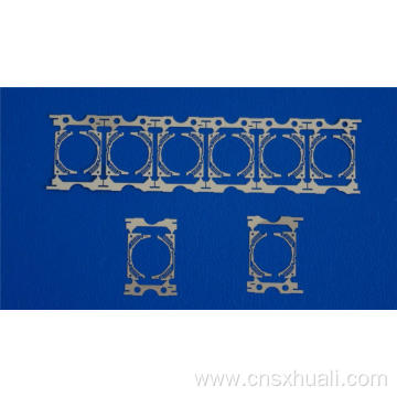
Now the etching technology has been widely used in the production of smart phone VCM springs, spacers and other products.
From Wikipedia, the free encyclopedia
The above is the Etching (Microfabrication) we have listed for you. You can submit the following form to obtain more industry information we provide for you.
You can visit our website or contact us, and we will provide the latest consultation and solutions
Send Inquiry
Most Popular
lastest New
Related Products
Send Inquiry
Privacy statement: Your privacy is very important to Us. Our company promises not to disclose your personal information to any external company with out your explicit permission.
Fill in more information so that we can get in touch with you faster
Privacy statement: Your privacy is very important to Us. Our company promises not to disclose your personal information to any external company with out your explicit permission.