
Payment Type:T/T
Incoterm:FOB,CIF,EXW
Min. Order:200 Piece/Pieces
Transportation:Ocean,Air,Express
Port:NINGBO,SHANGHAI
$0.01-10 /Piece/Pieces
Place Of Origin: China
Transportation: Ocean,Air,Express
Place of Origin: CHINA
Certificate: ISO9001:2015 / ISO14001:2015
Port: NINGBO,SHANGHAI
Payment Type: T/T
Incoterm: FOB,CIF,EXW
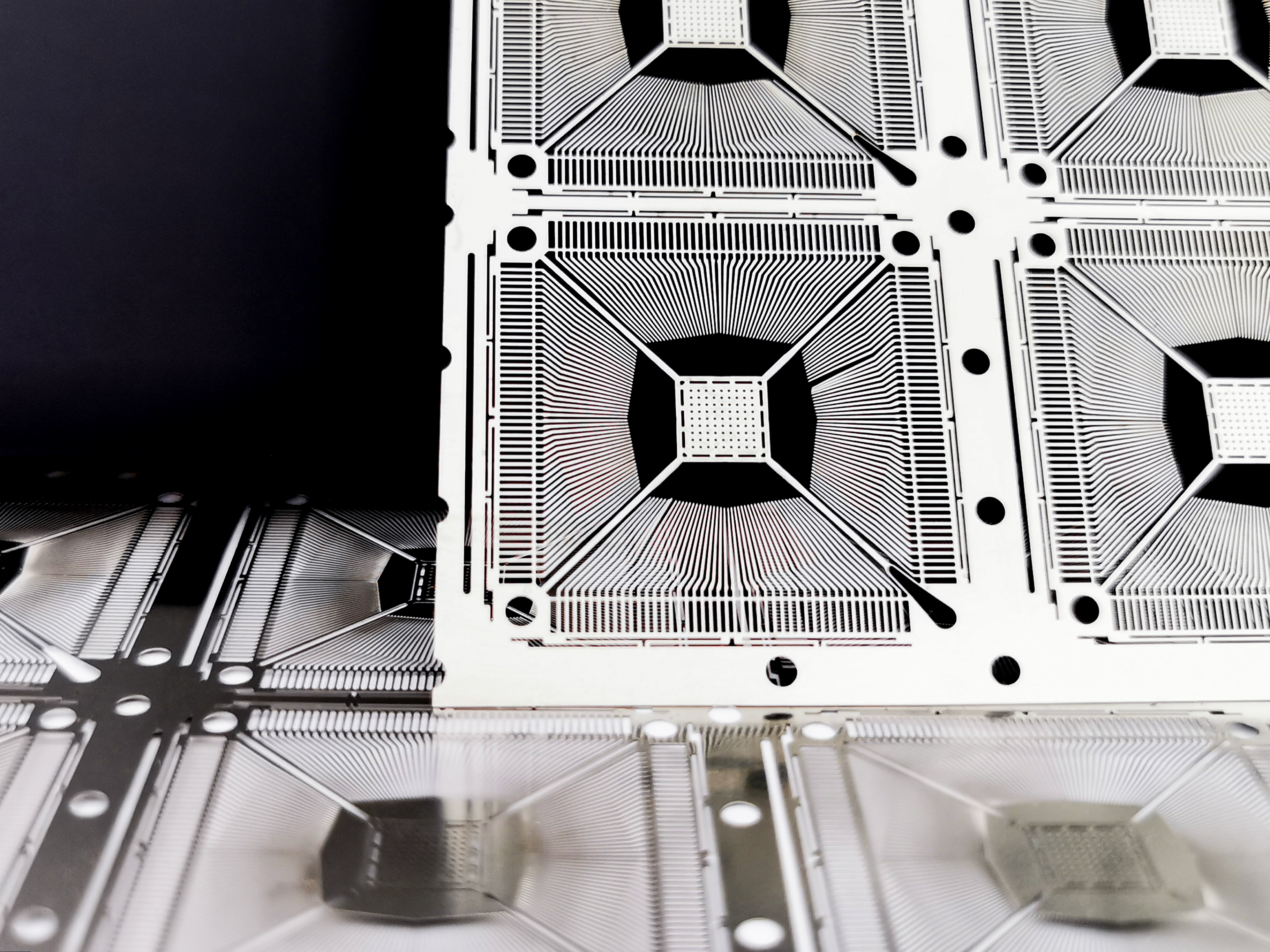
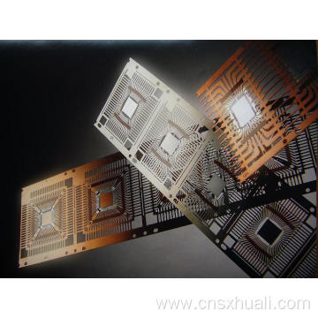
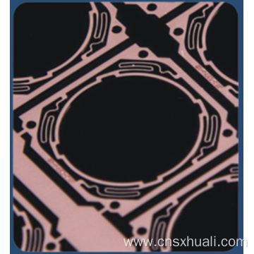
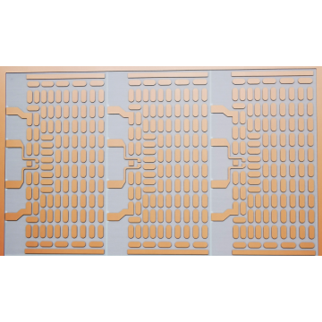
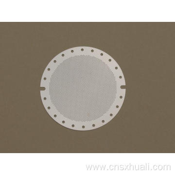
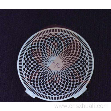
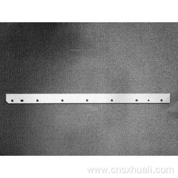
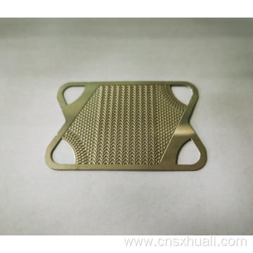
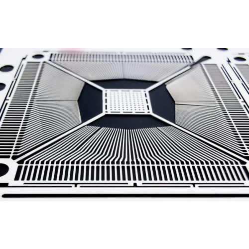
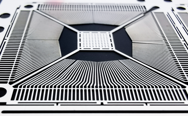
Etch High Precision Lead Frame for Semiconductor Packaging
IC Lead Frame is the basic material for semiconductor packaging, so it is widely used in emerging products such as artificial intelligence, Internet of Things, smart manufacturing and new energy vehicles. The material we use in IC Lead Frame is C192 or C194 Copper. The production of lead frames by metal etching process can achieve higher precision, for example, we can produce multi-pin (more than 100 pins) products of Smooth IC Lead Frame, and can also produce ultra-thin products, such as etched 0.125mm thickness products. Moreover, we can guarantee that our etched Copper IC Lead Frame have uniform arrangement, straight etching line and also the half etching product's surface is smooth and delicate.
Below are the specific parameters of this product, please check more IC lead frame in our website for more ideas.
| Material | Thickness | Minimum Diameter | Minimum Distance | Accuracy |
| C192/C194 Copper | 0.125mm - 0.25 mm | 0.05 mm | 0.18 mm - 0.3 mm | +- 0.02 mm —— +- 0.04 mm |
ETCH LEAD FRAME